

“Indirect Tax I Indirect Tax Litigation I Customs & FTP I Central Licensing I Arbitration I Advisory”
Dated: 21.09.2026
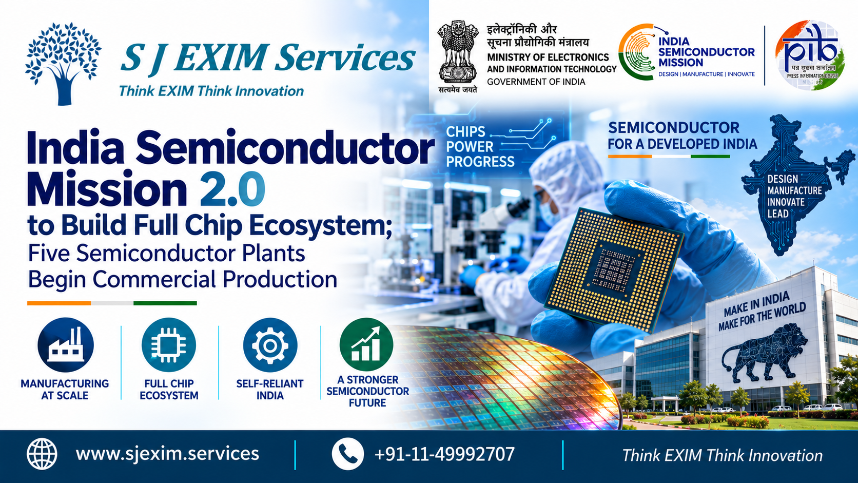
India Semiconductor Mission 2.0 to Build Full Chip Ecosystem; Five Semiconductor Plants Begin Commercial Production
India is moving into the next phase of its semiconductor strategy, with the Central Government outlining an expanded India Semiconductor Mission (ISM) 2.0 focused on developing a complete domestic ecosystem spanning chip design, semiconductor materials, manufacturing equipment, fabrication, OSAT/ATMP units and skilled manpower.
Speaking at SEMICON India 2026, Union Minister for Electronics and Information Technology Ashwini Vaishnaw said the semiconductor programme has moved from establishing the foundation of the industry to building an integrated ecosystem capable of competing globally.
According to the government release, five semiconductor manufacturing plants in India have already commenced commercial production, around 70,000 design engineers have been trained in four years, and the next phase will broaden its focus from chip design to system design and precision manufacturing.
ISM 2.0 to Focus on Complete Semiconductor Ecosystem
The Minister said the government’s semiconductor programme has entered a new phase.
While ISM 1.0 concentrated on establishing the foundational semiconductor ecosystem, ISM 2.0 is intended to take the industry forward across six key pillars:
Design; Materials and Machines; More Fabs; More ATMP Units; OSAT; and Talent.
- The government views the next phase as moving beyond individual manufacturing projects toward creating an interconnected domestic semiconductor value chain.
- Vaishnaw said ISM 1.0, originally envisaged as a six-year programme, achieved its objectives in four years. The government expects ISM 2.0 to progress on a similarly accelerated trajectory, supported by growing investor interest.
Five Semiconductor Manufacturing Plants Begin Commercial Production
- One of the most significant announcements in the release is that five chip manufacturing plants in India have commenced commercial production.
- The Minister said chips from these facilities are not only serving domestic requirements but are also being exported.
- According to the government, this demonstrates the emerging ability of semiconductor manufacturing in India to compete on cost and quality, both of which are critical for participation in the global semiconductor market.
- Demand for semiconductor products is currently strong, and several companies are expanding their production capacity.
- The release further states that a fab scheduled to be commissioned in 2028 already has a large part of its capacity booked, indicating advance demand for future domestic semiconductor capacity.
India Targets 200 Chip Design Companies Under ISM 2.0
- Chip design is expected to remain one of the central pillars of the next phase.
- Vaishnaw described India’s existing design capability—built through the country’s IT industry and global capability centres—as a major strength that can now be extended deeper into semiconductor development.
- The government estimates that at least 200 chip design companies could emerge under ISM 2.0, which the Minister described as a potential “game changer” for building homegrown semiconductor intellectual property.
- This signals that India’s semiconductor strategy is not confined to attracting fabrication facilities. It also seeks to develop domestic ownership and capability at the design and semiconductor-IP level.
Over 105 Chip-Design Startups Given Access to EDA Tools
- Under the first phase of the semiconductor programme, government support for chip-design startups focused partly on addressing the high cost of sophisticated Electronic Design Automation (EDA) tools.
- According to the release, more than 105 chip-design startups received access to state-of-the-art EDA tools through the programme.
- Of these, 20 startups received venture-capital funding.
- The government said the development of chips for actual products by participating startups has encouraged it to expand the programme and seek greater participation from larger companies as well as Indian-origin engineers working globally.
Precision Manufacturing and Applied R&D Become Next Priorities
- ISM 2.0 is also expected to have implications beyond semiconductor fabrication.
- The government says the broader electronics manufacturing ecosystem has helped build precision-manufacturing capabilities among Indian MSMEs, which are now serving industries including electronics, mobile manufacturing, aerospace, aviation, defence and semiconductors.
- The next priority identified by the Minister is applied research and development within manufacturing plants, particularly R&D aimed at improving product quality and manufacturing processes.
- The government also plans to develop a multi-level training model to create skilled manpower for precision manufacturing.
- This indicates a broader policy objective: semiconductor investment is being used not merely to create chip capacity but also to deepen India’s capabilities in high-precision industrial manufacturing.
70,000 Semiconductor Design Engineers Trained in Four Years
- Talent development forms another major pillar of the semiconductor strategy.
- India had initially set a target of training 85,000 semiconductor design engineers over 10 years. According to the government, approximately 70,000 design engineers have already been trained within four years.
- Students from around 400 engineering colleges, including institutions in smaller cities, have been provided access to industry-grade EDA tools.
- Students are also being given opportunities to take their designs through tape-out, allowing designs to move closer to actual semiconductor implementation and product development.
ISM 2.0 to Move Skills Beyond Chip Design to System Design
- The skilling strategy under ISM 2.0 is expected to broaden significantly.
- Rather than focusing predominantly on chip design, the government plans to move towards system design, with the stated objective of developing talent that is highly sought after by the semiconductor and electronics industries.
- Another emerging requirement is skilled manpower for cleanrooms and semiconductor plant maintenance.
- The government has indicated that its training target of one lakh technicians under ISM 2.0 may need to be increased depending upon industry demand.
- This is significant because semiconductor manufacturing requires not only highly specialised chip designers but also a large technical workforce for fabrication plants, cleanrooms, equipment maintenance, testing, packaging and precision manufacturing.
AI Server Manufacturing Emerging as Another Opportunity
- The semiconductor push is also being connected with India’s expanding electronics and artificial-intelligence infrastructure.
- Vaishnaw said electronics, semiconductors and AI applications are closely interconnected.
- According to the release, a manufacturing ecosystem for AI servers is emerging in India, with major server manufacturers showing interest in establishing manufacturing operations in the country.
- The government sees the development of components, finished products, laptops, servers and accessories as parts of a broader electronics ecosystem which, once sufficiently established, could support more consistent industrial growth.
Trust and IP Protection Seen as Key to Attracting Global Semiconductor Companies
- The Minister also highlighted trust and intellectual-property protection as important elements of India’s semiconductor investment proposition.
- India’s design capability, according to the government, provides an important advantage in strengthening the semiconductor ecosystem and increasing localisation.
- The release states that companies which had previously not established operations outside their home countries are now coming to India, which the government views as evidence of increasing confidence in India’s capabilities.
- For the semiconductor sector—where intellectual property, process technology, proprietary designs and supply-chain security are commercially critical—this element of the government’s strategy could be particularly important in attracting global investment.
From “Design in India” to “Design and Make in India”
- The government’s broader objective is to move India systematically towards becoming a product nation.
- Some chips being developed in India are already being used in strategic sectors, while semiconductor products are also being exported, according to the release.
- The government expects more “Design in India” and “Design and Make in India” products to emerge as the semiconductor programme progresses.
- The release also states that ATMP units are already exporting to Japan, while chips are being incorporated into products exported to the United States and European countries including Switzerland and Germany.
- This export dimension is important because it positions the semiconductor initiative not solely as an import-substitution programme, but as an attempt to integrate Indian semiconductor manufacturing into international value chains.
Why ISM 2.0 Matters for India’s Electronics Manufacturing Strategy
- The announcements at SEMICON India 2026 indicate a broadening of India’s semiconductor policy.
- The first phase concentrated heavily on creating the foundation: attracting investments, supporting chip-design startups, providing EDA infrastructure, approving semiconductor projects and developing skills.
ISM 2.0 is intended to move further into an ecosystem approach, linking:
semiconductor design → materials and manufacturing equipment → fabs → ATMP/OSAT → precision manufacturing → system design → skilled workforce → finished electronics products.
- This is particularly relevant because semiconductor and electronics supply chains are highly globalised. The government’s strategy appears aimed at increasing the portion of that value chain that can be undertaken within India while continuing to participate in international supply networks.
- Importantly, the release describes ISM 2.0 as the next phase and policy direction. Statements concerning future numbers of design companies, technician training and additional manufacturing capacity should therefore be understood as targets or expectations rather than completed outcomes.
Key Takeaway
India’s semiconductor programme is entering a broader phase in which the emphasis is shifting from establishing individual semiconductor projects to creating a full domestic semiconductor and electronics ecosystem.
With five semiconductor manufacturing plants commencing commercial production, approximately 70,000 design engineers trained, more than 105 chip-design startups receiving EDA access, and semiconductor-related exports already underway, the government is presenting ISM 2.0 as the next stage of industrial expansion.
The success of the next phase will depend on how the announced strategy translates into additional fabrication and packaging capacity, domestic materials and equipment capability, commercially viable Indian semiconductor IP, precision manufacturing, system design and a sufficiently skilled workforce.
In case you face any issues related to Indirect Tax-Customs, GST, Foreign Trade Policy (FTP), Arbitration matters and Central Licensing and related advisory matters in India then please feel free to get in touch with SJ EXIM Services.
We offer Legal advice and litigation support in matters related to Indirect Tax-Customs, FTP, other Indirect Tax matters & Arbitration law, all sorts of Central licensing and related matters. Come and explore the new way of doing business with us!
We specialize in paralegal services, litigation support, tax and regulatory matters, delivering reliable, efficient, and result-oriented legal assistance.
Source: Meity
Handy Download:
Connect with us for more-
@ Team S J EXIM SERVICES, New Delhi, IN
CP: Ms. Shubhra Jha, Founder
Tel: +91-11-4999 2707 I +91-9999005693
Web: www.sjexim.services
EMAIL: operations@sjexim.services I shubhra@sjexim.services
Facebook: www.facebook.com/sjeximservices
LinkedIn: https://www.linkedin.com/company/90794255/admin/feed/posts/
YouTube: https://www.youtube.com/@aadrikaalawindia
Subscribe our WhatsApp Channel: https://whatsapp.com/channel/0029VaTxDT8JZg4CHEOSoK47
Subscribe our Telegram Channel: https://t.me/sjeximindia







Leave a Reply